Today a wide variety of Lasers are used in several applications in the semiconductor industry. Laser technology is beginning to get integrated in major semiconductor processes including laser annealing, cutting, drilling, welding/bonding, debonding, marking, patterning, measurement, and deposition; driven by motherboards.
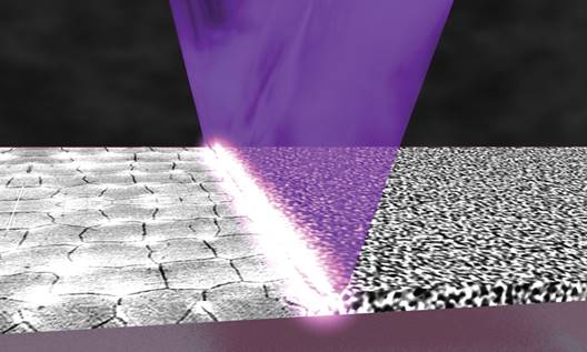
Semiconductor devices are built up in a series of nanofabrication processes performed on the surface of substrates made from highly pure single crystal silicon. These substrates are usually known as wafers. Excimer Laser-based annealing is the first process that is widely used in the fabrication of wafers. These thin wafers give photonic cutting tools an opportunity to gain a competitive edge over mechanical saw. The thinner the wafer, the faster a laser can dice it. Kerf widths and positioning tolerances are tighter, enabling street widths below 30 μm, instead of the usual 125 μm or more which is common with mechanical methods. Laser dicing systems also waste less silicon, so chip designers potentially gain more space to create more patterns.
LED technology provides further momentum to laser scribing applications. LEDs are grown on high-cost substrates, such as GaAs, Sapphire, GaP, and SiC, that only grow in value following epitaxy. Despite the common use of high-precision saws for dicing these devices, the use of blue emitters grown on sapphire has allowed UV laser systems to be developed, thanks to the hard nature of Sapphire and the low cost of consumables involved with traditional mechanical dicing.
Laser Lift-off (majorly Excimer laser-based) is another exciting process used in the fabrication of LEDs. Depending on the application and type of device, lasers’ powers can be modulated, which makes them useful for a wide range of applications.
Lasers can also be used to make tiny markings on sensitive equipment, which makes them ideal for semiconductor manufacturing. The two main reasons why the laser marking process is important are, traceability and readability. There are two main types of lasers used for marking of this kind: near-infrared (NIR) and green lasers. Both are well-suited to the job, but they differ in some fundamental ways.
Near-Infrared Laser: The near-infrared laser is extremely versatile, making it ideal for a wide range of machine applications like semiconductor manufacturing. Its effectiveness is due to the energy range falling within the spectral range needed to mark wafers.
Green Lasers: On the other hand, Green lasers are the result of second-harmonic generation processes, also known as frequency doubling.
Each step of the semiconductor manufacturing process is important for achieving a high-quality result. However, the choice of the most suitable laser processing type depends strongly on the material to be processed, processing parameters, and the manufacturing process step.
Compact and highly functional electronics are driving the semiconductor industry to produce smaller devices on thinner wafers and with new materials. Laser micromachining increasingly presents a solution to cutting, dicing, and scribing of microelectronic devices built on silicon and similar substrates, particularly as new chip and package designs emerge in the next decade.
Ankit Singhal
Laser Science Pvt Ltd

0 Comments